CMOS Process
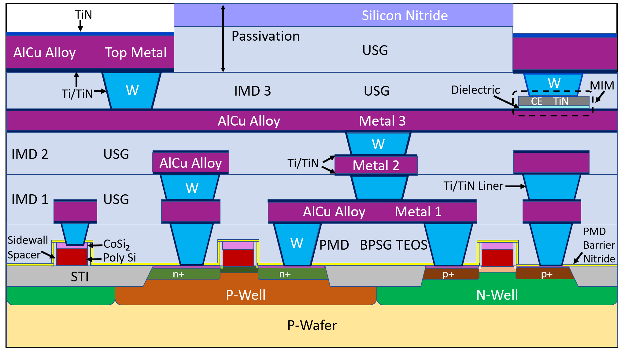
SCL has standard 180nm CMOS baseline process technology. It enables the development of single- or dual-voltage circuits requiring 1.8V, 1.8/3.3V, or 1.8V/5V power- supplies using its dual-gate oxide process, which features 4-6 Al-metal layers with thick-last metal. The process has add-on modules, namely 1.8V-HVt-transistors for low leakage, high-density precision MIM capacitors (1 or 1.7 or 2.8fF/um2), high-resistance poly (1 and 2 Kohms/sq.), Deep N-well for noise isolation, and more.
Baseline Process Technology Features
- 1.8V Core CMOS.
- 1.8V or 3.3V I/O.
-
Single poly & upto 6 Metal Layers with USG-BEOL.
-
23-34 Mask layers (depending on Metal Layers and Analog modules).
Analog Process Modules
-
High-Vt (Low leakage current ~one order less).
-
Metal Insulator Metal capacitor: Single MIM (1 & 2fF/µm2) & stacked MIMs (2x).
-
Deep N-Well (Isolated p-wells for substrate noise isolation).
-
High resistance poly silicon resistor: HIPO (1kΩ/sq; 2kΩ/sq).
- Thick Last metal (2µm).
- 5V-MOSFETs (Gox: 110A).
CMOS Process Features
- 8” p-type Silicon (1-2 Ω-cm).
- Shallow Trench Isolation (STI).
- Retrograde wells.
-
Dual gate oxide (Nitrided gate oxide: 30A:1.8V & 70A:3.3V/110A:5V).
-
Dual gate poly (p+ doped for PMOS & n+ doped for NMOS).
-
Salicide (Cobalt Silicide for S/D & gate poly).
- Tungsten(W) Fill contacts/Vias.
-
Ti/TiN/AlCu/Ti/TiN metal interconnects.
-
High density plasma oxide, USG (k=4.2) as Inter Metal Dilectric (IMD).
-
CMP for STI, ILD/IMD, Tungsten Contacts/Vias.
-
DUV (248nm) with Rule based OPC & MUV (365nm) lithography for critical & non-critical layers.
Software
-
Cadence Suite
-
Sentaurus TCAD
-
Silvaco TCAD
-
Keysight IC-CAP
-
xCalibrate
CMOS Fabrication Facility
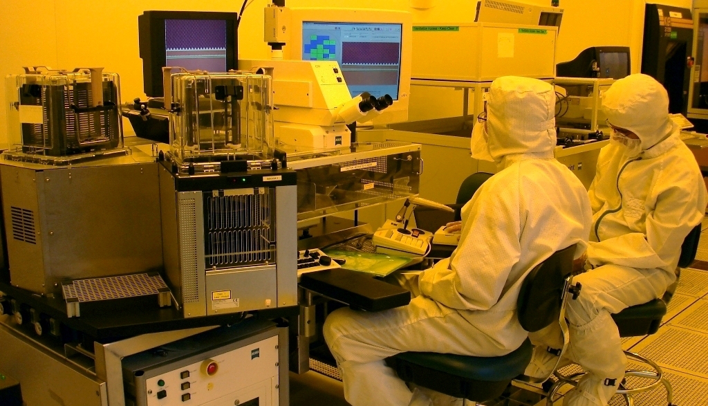
SCL has 8” wafer fab line @180 nm CMOS technology node for the fabrication of products in analog, digital, mixedsignal, memory, optoelectronics and MEMS devices. The facility meets international standards in terms of design, process equipment, in-line inspection & metrology tools, and support utilities. Fab has cleanrooms of class 1, 10, 100, and 1000 with controlled environmental conditions. SCL process is qualified as per JP-001A standard.
-
180 nanometer CMOS Process for Fabrication of products in Digital, Mixed Signal and Analog domains.
-
Process Equipment Line, In-line Inspection & Metrology Tools and Support Utilities as per international standards.
-
Clean Rooms of Class 1, 10, 100 and 1000 with controlled environmental conditions.
-
Dedicated bays for Wafer Fabrication Processes viz. Diffusion, Lithography, Etching (Dry & Wet), Implantation, Thin Films working seamlessly from Wafer-in to Wafer-out.
-
BKMs (Best Known Methods) comprising regular Tool QCs, Preventive Maintenance and Process Control & Monitoring through in-line defect inspection & measurement through Metrology Tools as per industry standards.
-
Commensurate with the requirements of Fab Lines and other process areas, support infrastructure namely Utility Plants, High Purity Systems and distribution Networks operate on 24x7 basis to maintain uninterrupted supplies of various Utilities viz. Ultra-Pure water, Bulk & Speciality Gases, Clean Power, etc..