MEMS Process
At SCL, the fabrication line handles 150-mm (6")-diameter different substrates like double-sided polished Silicon wafers, Epi-wafers, SOI wafers, and high-resistive Silicon wafers. All the basic fabrication steps that are derived from standard CMOS technology, viz., lithography, deposition, ion implantation, and etching, are available in the class-10 environment.
Salient features of MEMS Process
BULK MICRO-MACHINING
- Aspect ratios of ~10:1 and 90±2° profiles with DRIE
- Selectivity with PECVD Oxide 250: 1
- Etch rate > 5 um/min for an exposed area of 30%
- For more design flexibility and high throughput etching at other angles such as 54.7° using KOH
SURFACE MICRO-MACHINING
- PSG as sacrificial for wet release followed by CPD (for Poly as structural material) & VHF
- Photoresist as sacrificial layer for dry release (for Metal as structural material)
MEMS SPECIFIC THIN FILMS
- Low stress Silicon Nitride
- Doped and Undoped Poly Silicon
- PSG/BPSG (Low temperature)
MEMS SPECIFIC LITHOGRAPHY
- Lift- off process
- Front to Back contact 1:1 Aligner
- High Aspect Ratio Lithography with Negative Resists
- Polyimide coating
BONDING
- Eutectic (Au-Si, Au-SiO) bonding
- Anodic Bonding for Si-Glass wafers
- Thermocompression Bonding
- Fusion Bonding
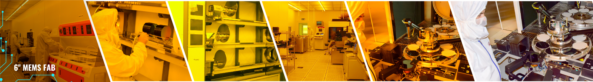
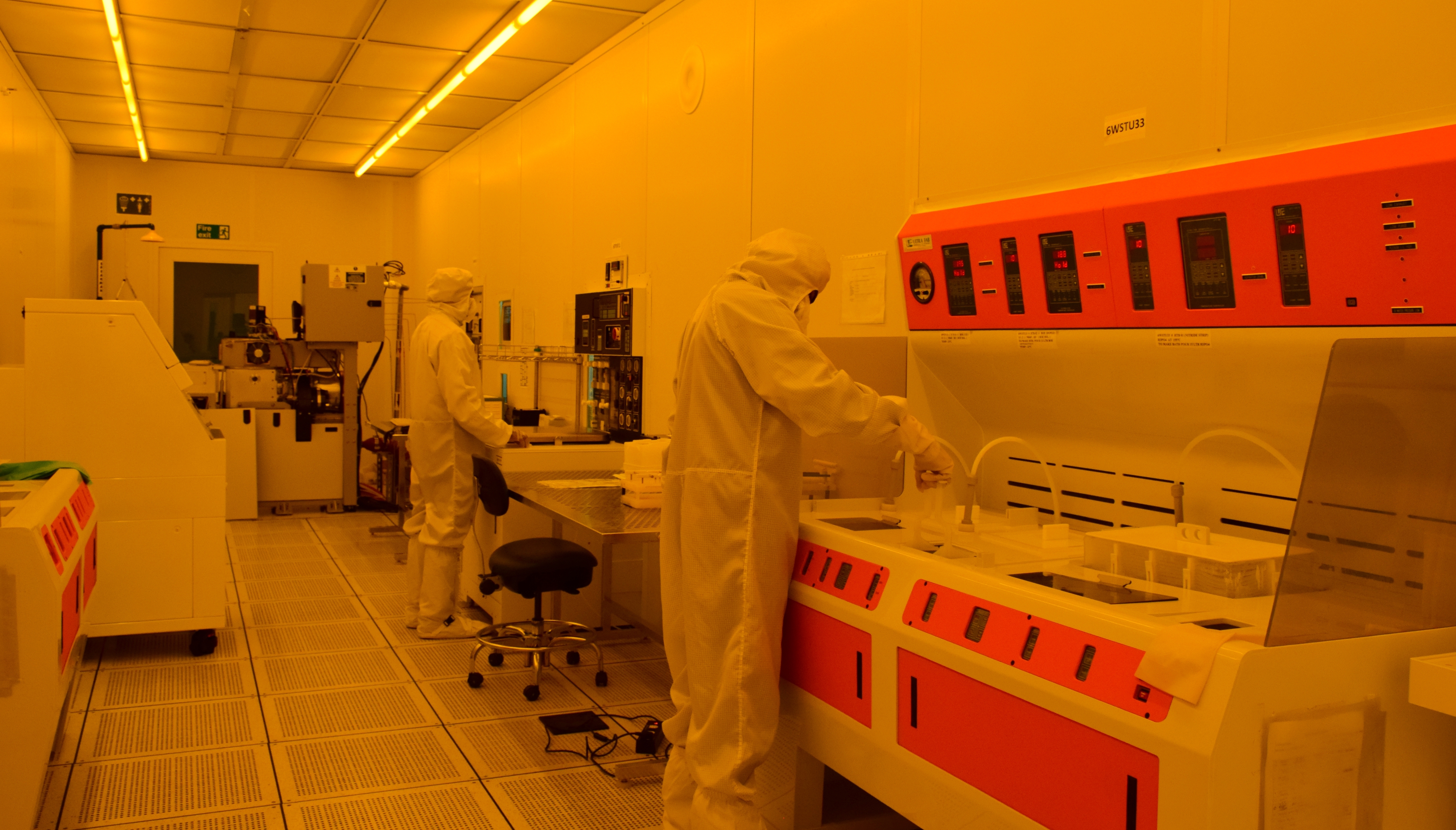
MEMS Fabrication Facility
SCL has state-of-the-art 6” fab line for MEMS based devices and detector development and is expanding it to include a compound semiconductor fabrication facility for the production of optoelectronic and high-power devices. The key features are:
-
6” Process Equipment Line, In-line Inspection & Metrology Tools and Support Utilities as per international standards.
-
Clean Rooms of Class 10 & Class 100 (Post CMOS) with controlled environmental conditions.
-
Dedicated bays for Wafer Fabrication Processes viz. Diffusion (High temperature furnaces), Lithography (5X stepper, 1X aligner, coater developer track), Etching (Dry & Wet), Implantation ( High and medium current implanters), Thin Films (PVD & CVD furnaces for dielectrics and metals) working seamlessly from Wafer-in to Wafer-out.
-
MEMS Specific fabrication capabilities like wafer bonding, electroplating, glass wafer processing, Vapor HF, CPD etc.
-
Characterization facility including Laser Doppler Vibrometer, Nanoindentor, AFM, XRD, 4 Point Probe resistance measurement.
MEMS Multi Project Wafer (MMPW) Programme
MMPW programme is designed in such a way that to provide low cost, easy access to foundry services to reduce the overall time and effort in developing MEMS devices. Currently MMPW is aimed to give access to three distinct areas:
-
SOI-MMPW :- SOI-MMPW (8-mask process) is targeted to fabricate devices using Silicon-On-Insulator bulk micromachining technology.
-
PIEZO-MMPW :- PIEZO-MMPW (6-mask process) is designed for general purpose micromachining of piezoelectric devices in SOI framework.
-
POLY-MMPW :- POLY-MMPW (6-mask process) is a two-layer Polysilicon surface micromachining process. For each of the above categories, dedicated process flow is developed.
Software
-
Ansys
-
HFSS
-
Coventor
-
Intellisuite
-
COMSOL